KINGYOUP Laser Debonding System KINGYOUP Sputtering System
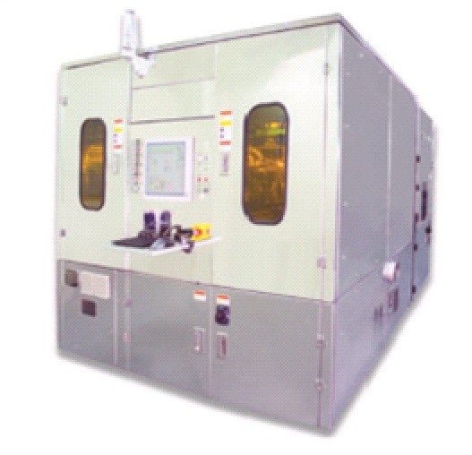
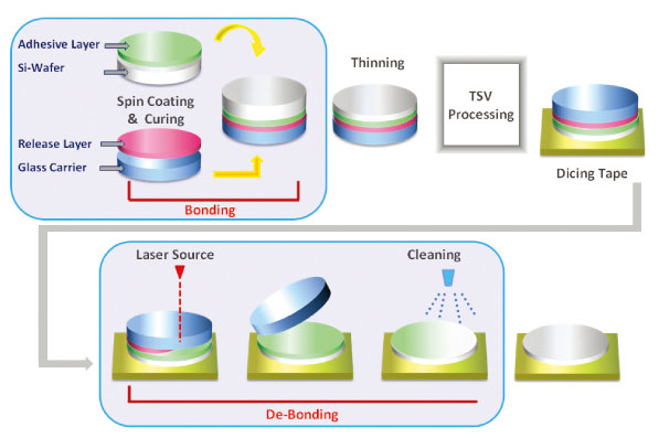
Laser Debonding System for Temporary Bonding
Video
- High throughput
- The laser minimizes the cost of operation and maintenance
- Fast release from low power laser
- Full absorption by the coating layer without defect
- Minimum de-bonding stress
- Special release layer
- More adhesive options
Standard Product(s)
LD- Semi Automatic 200/300● Equipment Dimension: 1,600mm(W)*1,200mm(D)*2,430mm(H)
● Max. Scan Area: 470mm*470mm (4” /8” /12” wafer compatible)
● Scan Time:
1. 4”: 15 sec/wafer
2. 8”: 35 sec/wafer
3. 12”: 70 sec/wafer
LD- Automatic 200/300
● Equipment Dimension: 2,660mm(W)*2,800.5mm(D)*2,087mm(H)
● Max. Scan Area: 470mm*470mm (4” /8” /12” wafer compatible)
● WPH
1. 4”: 55 wafers/hour
2. 8”: 42 wafers/hour
3. 12”: 30 wafers/hour
Applications
- 2.5D/3D IC TSV
- Chip on Wafer on Substrate (CoWoS)
- Fan Out Wafer Level Package (FOWLP)
- Glass Interposer
- CIS BSI
- III V, RF Compound
- Vertical LED
- Flexible Film Substrate Handling
- Thin Glass Handling
- Panelized TOL
De-Bonding Process Flow